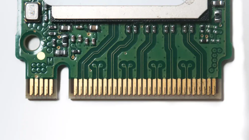
As a cutting-edge technology in the manufacturing of Printed Circuit Boards (PCBs), PCB edge plating not only plays a crucial role in enhancing the reliability of circuit boards but is also gaining increasing attention in high-frequency and high-speed applications. This article aims to provide a professional analysis of the PCB edge plating technology, exploring its process, rationale, material selection, and its application advantages.

Substrate Preparation: In the early stages of PCB manufacturing, the substrate undergoes preparation, involving surface treatment and precise dimensional design.
Mask Application: A mask is applied using a photoresist technique to ensure that only the edge area is affected by the plating process.
Gold or Nickel Plating: The PCB is immersed into a plating bath where, through electrochemical reactions, selective gold or nickel plating is carried out on the edge region to improve conductivity and corrosion resistance.
Mask Removal: After plating, the mask is removed using a chemical solvent, leaving the plated layer only on the edge area.
Cleaning and Coating: Rigorous cleaning of the PCB removes residual plating solution, followed by surface coating of the edge area to enhance corrosion resistance.
Enhancing Reliability: By increasing the conductivity of the edge area, PCB edge plating significantly improves the overall reliability of the circuit board, particularly in high-frequency and high-speed circuits.
Corrosion and Oxidation Prevention: The selectively applied metal layer effectively prevents corrosion and oxidation of the edge area, which is more susceptible to environmental influences.
Improved Connectivity: PCB edge plating establishes robust connections in the region of slots or connectors, enhancing connectivity and overall mechanical strength.
Metal Materials: Choosing high-quality metal materials, such as gold or nickel, ensures that the plated layer exhibits excellent conductivity and corrosion resistance.
Mask Material: Employing high-temperature and chemically resistant mask materials, such as UV-cured resins, ensures the stability of the mask throughout the process.
This professional analysis of PCB edge plating technology underscores its irreplaceable role in improving circuit board performance, reliability, and durability. A comprehensive understanding of its process and principles empowers professionals in the electronics manufacturing industry to effectively apply this technology, driving its future development and innovation.
WeChat
Scan the QR Code with WeChat