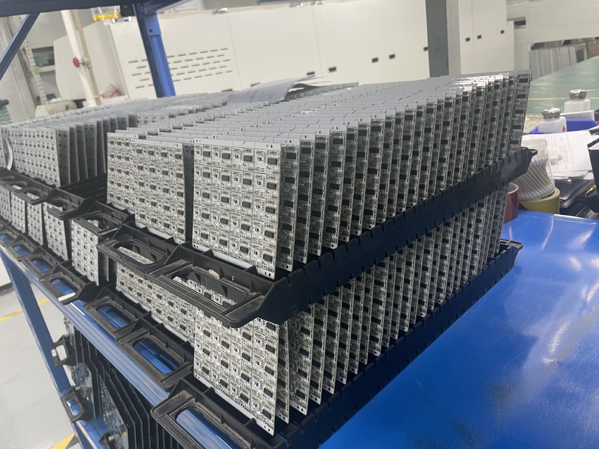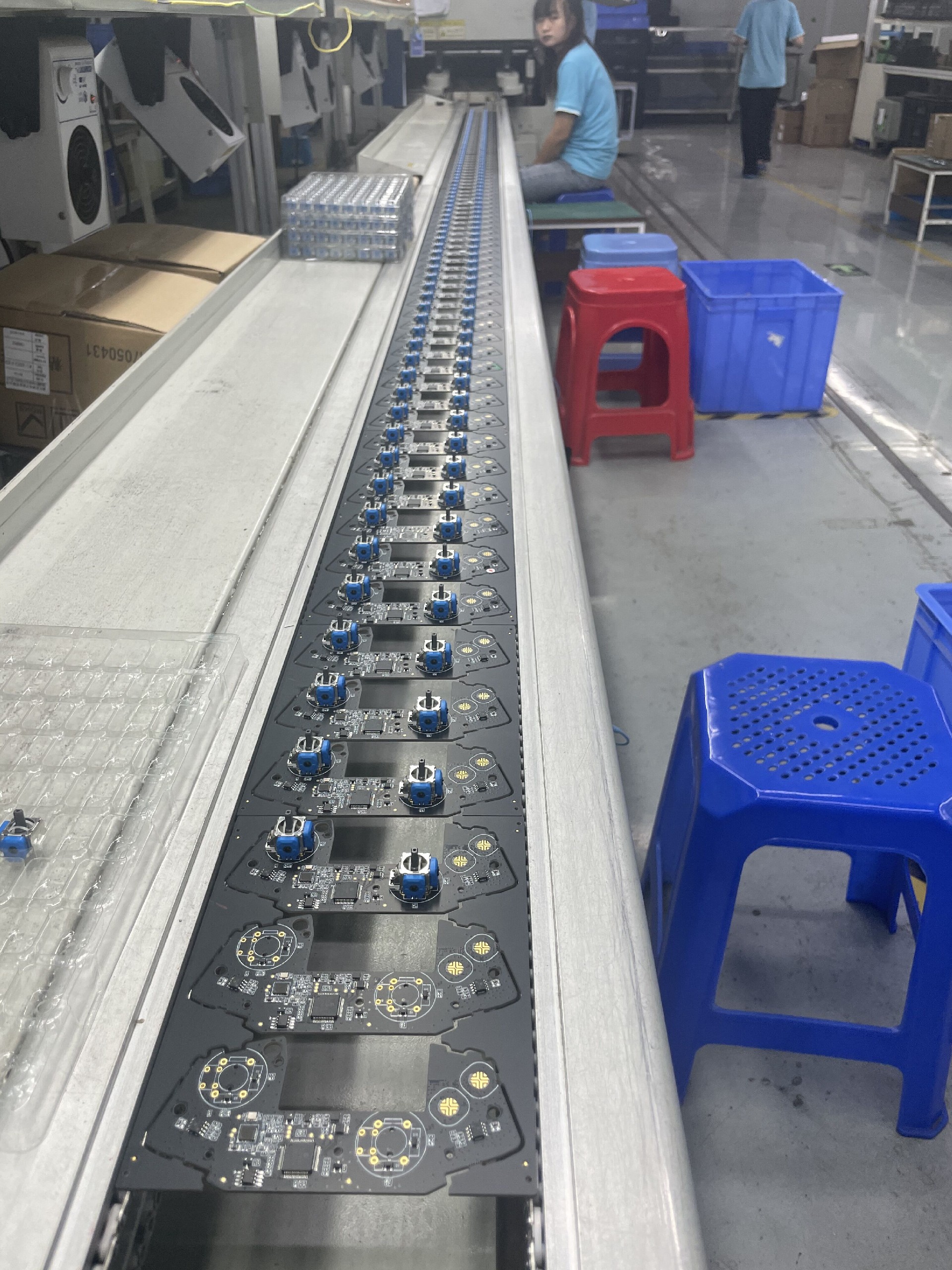
Multi board PCB design is a design method that includes multiple independent circuit boards in a single PCB project. Each independent circuit board is typically referred to as a sub board or module. These sub boards are physically separated, but connected to the motherboard through connectors, wiring harnesses, or other interconnections. The entire design forms a fully functional system.

Modular design: Decompose the entire system into independent modules, each corresponding to an independent PCB sub board. This design allows each sub board to be independently designed, tested, and manufactured.
Simplify maintenance and upgrades: As the system is divided into multiple modules, it is easier to replace or upgrade individual sub boards during maintenance and upgrades without modifying the entire system.
Reducing electromagnetic interference: Physical isolation between modules can reduce the propagation of electromagnetic interference and improve the electromagnetic compatibility of the system.
Easier parallel development: Different sub boards can be designed by different teams simultaneously, thereby shortening the development cycle of the entire project.
Suitable for large systems: For large electronic systems, multi board design provides an effective organizational structure, making the system more manageable.
Flexible customization: Users can choose different combinations of sub boards to customize system configurations that meet their needs.
In multi board PCB design, the motherboard usually includes the main system control circuit and interfaces for communication with various sub boards. The sub board is responsible for specific functions, such as power management, sensor interfaces, communication modules, etc. The interconnection methods can be sockets, connectors, flexible cables, etc., depending on the specific requirements of the system.

The working principle of multi board PCB design is based on decomposing the entire system into independent sub boards, each responsible for specific functions. These sub boards are connected to the motherboard through connectors, wiring harnesses, or other interconnections, forming a complete electronic system. The following is the basic working principle of multi board PCB design:
The system designer divides the entire system into multiple independent modules or sub boards based on system functionality and requirements. Each sub board undertakes a specific function in the system.
Design each sub board independently. This includes circuit design, layout design, component selection, etc. The design of each sub board can be handled by different teams or designers to achieve parallel development.
Determine the physical connection method between daughter boards, usually using sockets, connectors, wiring harnesses, etc. This ensures electrical connections and communication between the daughter boards.
The motherboard contains the main control circuits, interface circuits, and interfaces for communication with each sub board of the system. The connectors and interfaces on the motherboard allow for connection to each daughter board.
Define the communication protocol between each sub board and the motherboard. This ensures that the sub boards can work together, transmit information, and execute the functions of the entire system.
Design appropriate power management circuits for each sub board. This includes power supply voltage, current distribution, etc. to ensure that each sub board receives the correct power supply.
Physically insert each sub board into its corresponding slot or connector on the motherboard to form a complete system. The sub boards are electrically connected through connectors.
Design and develop corresponding software for the entire system to ensure effective communication and collaborative work between the motherboard and various sub boards.
Test and debug the entire system. This includes verifying the functionality of each sub board, ensuring normal communication between each sub board, and ensuring that the performance of the entire system meets the design requirements.
When it is necessary to maintain or upgrade the system, specific sub boards can be replaced or upgraded more easily without affecting the normal operation of the entire system.
Through this working principle, multi board PCB design achieves modular, maintainable, scalable, and highly flexible design of the system, providing an effective method for the development of complex electronic systems
Welcome to contact us to customize your unique multi board PCB design! Our team is committed to providing customers with highly customized electronic solutions to meet the needs of various complex systems. Regardless of the scale of your project, we can provide innovative multi board PCB designs to ensure system modularity, maintainability, and high flexibility.
WeChat
Scan the QR Code with WeChat